Related Resources: Design for Manufacturing
Testability Primer, JTAG IEEE std 1149.1
Design for Manufacturability
Engineering Applications and Design
Testability Primer, JTAG IEEE std 1149.1
Design for Test (DFT), also known as design for testability, is a process that incorporates rules and techniques in the design of a product to make testing easier.
Open: Testability Primer, JTAG IEEE std 1149.1
Minimum Free Membership Account Required
Introduction: Structured design for test is a system methodology rather than a collection of discrete techniques. This methodology impacts all phases of a product’s life, from device circuit design through field service. Design for test is used to manage complexity, minimize development time, and reduce manufacturing costs.
Testing has two major aspects: control and observation. To test any system it is necessary to put the system into a known state, supply known input data (test data), and observe the system to see if it performs as designed and manufactured. If control or observation cannot be carried out, there is no way to know empirically if the system performs as it should.
During the normal product development flow, testing (it may be known by different names) takes place at many points during the process. If testing is considered at the chip design level, its benefits can be used at all levels of electronic assembly, from chip through system level. See Figure 1.
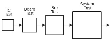
Figure 1
Chip Through System-Level Test
Designers usually test various functions to validate their design. Manufacturing and customer groups subject the design to an assortment of unique criteria to see if the concept works in practice. Is it manufacturable? Will it stand up to real-world operating conditions? Will repair be cost efficient? In addition to direct testability considerations, production managers want features designed into the product to help them minimize scrap and manufacturing costs. Good system-testability methodology provides an integrative function throughout the product development cycle and allows materials created during an early phase of development to be reused in later phases. Various chip designers have used this integration feature as a tool to help manage the development of complex products.
Testability provides companies with a firmer grasp on the economic and market-window constraints due to product development. One major workstation manufacturer claimed:
- Test program development would have been nearly impossible without scan techniques.
- Chip-level test development time fell from 1 man-year to about 20 hours.
- Board-level test development time fell from multiple man-years to about a week.
- Three months were cut off development time.
TOC
Introduction 1-1 . . . . . . . . . . . . . . . . . . . . . . . . . . . . . . . . . . . . .
Overall Rationale for Design for Test 1-2 . . . . . . . . . . . . . . . . .
Reduced Cost and Higher Quality 1-3 . . . . . . . . . . . . . . . . . . .
Benefits Over Standard Test Methods 1-3 . . . . . . . . . . . . . . . .
Standard Test Solutions Versus Proprietary Solutions 1-5 . . .
An Industry Standard — IEEE Std 1149.1-1990
(JTAG) 1-5 . . . . . . . . .
Benefits of Testability 2-1 . . . . . . . . . . . . . . . . . . . . . . . . . . . . .
Traditional Testing 2-1 . . . . . . . . . . . . . . . . . . . . . . . . . . . . . . . . .
Efficient Testing 2-1 . . . . . . . . . . . . . . . . . . . . . . . . . . . . . . . . . . .
Lower Cost for Testing 2-1 . . . . . . . . . . . . . . . . . . . . . . . . . . . . .
Production Time Savings 2-2 . . . . . . . . . . . . . . . . . . . . . . . . . . .
Easier Board-Level Isolation 2-2 . . . . . . . . . . . . . . . . . . . . . . . .
Simple Access to Circuits 2-2
Boundary-Scan Architecture
and IEEE Std 1149.1 3-1 . . . . . . . . . . . . . . . . . . . . . . . . . .
Boundary-Scan Overview 3-2 . . . . . . . . . . . . . . . . . . . . . . . . . . .
Test Interface and Boundary-Scan Architecture 3-3 . . . . . . . .
Test Access Port and Operation 3-5 . . . . . . . . . . . . . . . . . . . . .
IEEE Std 1149.1 Registers 3-8 . . . . . . . . . . . . . . . . . . . . . . . . . .
Instruction Register (Required) 3-8 . . . . . . . . . . . . . . . . . .
Data Registers 3-9 . . . . . . . . . . . . . . . . . . . . . . . . . . . . . . .
IEEE Std 1149.1 Required Instructions 3-12 . . . . . . . . . . . . . .
BYPASS Instruction 3-12 . . . . . . . . . . . . . . . . . . . . . . . . . .
SAMPLE/PRELOAD Instruction 3-12 . . . . . . . . . . . . . . . .
EXTEST Instruction 3-13 . . . . . . . . . . . . . . . . . . . . . . . . . .
IEEE Std 1149.1 Optional Instructions 3-13 . . . . . . . . . . . . . . .
INTEST Instruction 3-13 . . . . . . . . . . . . . . . . . . . . . . . . . . .
RUNBIST Instruction 3-13 . . . . . . . . . . . . . . . . . . . . . . . . .
CLAMP Instruction 3-13 . . . . . . . . . . . . . . . . . . . . . . . . . . .
HIGHZ Instruction 3-14 . . . . . . . . . . . . . . . . . . . . . . . . . . . .
IDCODE Instruction 3-14 . . . . . . . . . . . . . . . . . . . . . . . . . .
USERCODE Instruction 3-14 . . . . . . . . . . . . . . . . . . . . . . .
Obtaining IEEE Std 1149.1-1990 3-15Using DFT in ASICs 4-1 . . . . . . . . . . . . . . . . . . . . . . . . . . . . . .
Design-for-Test Considerations 4-1 . . . . . . . . . . . . . . . . . . . . . .
The Need for Testability 4-2 . . . . . . . . . . . . . . . . . . . . . . . . . . . .
Test-Time Cost 4-3 . . . . . . . . . . . . . . . . . . . . . . . . . . . . . . . . . . . .
Time to Market 4-3 . . . . . . . . . . . . . . . . . . . . . . . . . . . . . . . . . . . .
Fault Coverage and Cost of Ownership 4-5 . . . . . . . . . . . . . . .
Developing Testability Strategies 4-8 . . . . . . . . . . . . . . . . . . . .
Data Formats 5-1 . . . . . . . . . . . . . . . . . . . . . . . . . . . . . . . . . . . .
Boundary-Scan Description Language (BSDL) 5-1 . . . . . . . .
How BSDL Is Used 5-1 . . . . . . . . . . . . . . . . . . . . . . . . . . . .
Elements of BSDL 5-2 . . . . . . . . . . . . . . . . . . . . . . . . . . . .
Verifying BSDL Accuracy 5-4 . . . . . . . . . . . . . . . . . . . . . . .
Potential BSDL Errors 5-5 . . . . . . . . . . . . . . . . . . . . . . . . .
How to Receive the BSDL Specification 5-5 . . . . . . . . . .
Obtaining BSDL for TI Devices 5-5 . . . . . . . . . . . . . . . . . .
Hierarchical Scan Description Language (HSDL) 5-6 . . . . . .
Elements of HSDL 5-6 . . . . . . . . . . . . . . . . . . . . . . . . . . . .
How to Receive the HSDL Specification 5-8 . . . . . . . . . .
Serial Vector Format (SVF) 5-9 . . . . . . . . . . . . . . . . . . . . . . . . .
SVF Structure 5-10 . . . . . . . . . . . . . . . . . . . . . . . . . . . . . . .
Default State Transitions 5-12 . . . . . . . . . . . . . . . . . . . . . .
SVF Example 5-15 . . . . . . . . . . . . . . . . . . . . . . . . . . . . . . .
How to Receive the SVF Specification 5-16 . . . . . . . . . .
Suggested Design-for-Test Flow 6-1 . . . . . . . . . . . . . . . . . . .
Test Requirements 6-2 . . . . . . . . . . . . . . . . . . . . . . . . . . . . . . . .
Built-In Self-Test (BIST) Methodology 6-3 . . . . . . . . . . . . . . . .
Internal Scan Test Methodology 6-3 . . . . . . . . . . . . . . . . . . . . .
Design Effort 6-4 . . . . . . . . . . . . . . . . . . . . . . . . . . . . . . . . . . . . . .
IC Design Implementation 6-4 . . . . . . . . . . . . . . . . . . . . . .
IC Simulation 6-6 . . . . . . . . . . . . . . . . . . . . . . . . . . . . . . . . .
Using SVF for IC Design Validation 6-6 . . . . . . . . . . . . . .
Data Passed to Board Designer 6-7 . . . . . . . . . . . . . . . . .
Board Design 6-8 . . . . . . . . . . . . . . . . . . . . . . . . . . . . . . . . . . . . .
Constraints 6-8 . . . . . . . . . . . . . . . . . . . . . . . . . . . . . . . . . . . . . . .
Partitioned Scan Path 6-8
Board Validation/Manufacturing Test 6-9 . . . . . . . . . . . . . . . . .
Summary 6-10 . . . . . . . . . . . . . . . . . . . . . . . . . . . . . . . . . . . . . . . .
Applications 7-1 . . . . . . . . . . . . . . . . . . . . . . . . . . . . . . . . . . . . .
Board-Etch and Solder-Joint Testing 7-1 . . . . . . . . . . . . . . . . .
Solution 7-1 . . . . . . . . . . . . . . . . . . . . . . . . . . . . . . . . . . . . .
Detailed Description 7-2 . . . . . . . . . . . . . . . . . . . . . . . . . . .
Summary 7-4 . . . . . . . . . . . . . . . . . . . . . . . . . . . . . . . . . . . .
Cluster Testing 7-5 . . . . . . . . . . . . . . . . . . . . . . . . . . . . . . . . . . . .
Solution 7-5 . . . . . . . . . . . . . . . . . . . . . . . . . . . . . . . . . . . . .
Detailed Description 7-5 . . . . . . . . . . . . . . . . . . . . . . . . . . .
Summary 7-6 . . . . . . . . . . . . . . . . . . . . . . . . . . . . . . . . . . . .
Board-Edge Connector Testing 7-7 . . . . . . . . . . . . . . . . . . . . . .
Solution 7-7 . . . . . . . . . . . . . . . . . . . . . . . . . . . . . . . . . . . . .
Detailed Description 7-7 . . . . . . . . . . . . . . . . . . . . . . . . . . .
Summary 7-9 . . . . . . . . . . . . . . . . . . . . . . . . . . . . . . . . . . . .
ASIC Verification 7-10 . . . . . . . . . . . . . . . . . . . . . . . . . . . . . . . . .
Solution 7-10 . . . . . . . . . . . . . . . . . . . . . . . . . . . . . . . . . . . .
Detailed Description 7-10 . . . . . . . . . . . . . . . . . . . . . . . . . .
Summary 7-11 . . . . . . . . . . . . . . . . . . . . . . . . . . . . . . . . . . .
Memory-Testing Techniques 7-12 . . . . . . . . . . . . . . . . . . . . . . .
Solution 7-12 . . . . . . . . . . . . . . . . . . . . . . . . . . . . . . . . . . . .
Detailed Description 7-12 . . . . . . . . . . . . . . . . . . . . . . . . . .
Summary 7-16 . . . . . . . . . . . . . . . . . . . . . . . . . . . . . . . . . . .
Backplane Multidrop Environment 7-17 . . . . . . . . . . . . . . . . . .
Solution 7-19 . . . . . . . . . . . . . . . . . . . . . . . . . . . . . . . . . . . .
Detailed Description 7-20 . . . . . . . . . . . . . . . . . . . . . . . . . .
Summary 7-21 . . . . . . . . . . . . . . . . . . . . . . . . . . . . . . . . . . .
Embedded Applications 7-21 . . . . . . . . . . . . . . . . . . . . . . . . . . .
Solution 7-21 . . . . . . . . . . . . . . . . . . . . . . . . . . . . . . . . . . . .
Detailed Description 7-21 . . . . . . . . . . . . . . . . . . . . . . . . . .
Summary 7-23 . . . . . . . . . . . . . . . . . . . . . . . . . . . . . . . . . . .
Boundary-Scan Test Flow 7-24 . . . . . . . . . . . . . . . . . . . . . . . . .
Solution 7-24 . . . . . . . . . . . . . . . . . . . . . . . . . . . . . . . . . . . .
Detailed Description 7-24 . . . . . . . . . . . . . . . . . . . . . . . . . .
Summary 7-28
Product Summary 8-1 . . . . . . . . . . . . . . . . . . . . . . . . . . . . . . . .
IEEE Std 1149.1-Compatible Components 8-1 . . . . . . . . . . . .
Highlights 8-1 . . . . . . . . . . . . . . . . . . . . . . . . . . . . . . . . . . . .
IEEE Std 1149.1 (JTAG) Boundary-Scan Logic 8-2 . . . . . . . .
Bus Interface 8-3 . . . . . . . . . . . . . . . . . . . . . . . . . . . . . . . . .
Universal Bus Transceiver (UBT) 8-4 . . . . . . . . . . . . . .
Scan Support 8-5 . . . . . . . . . . . . . . . . . . . . . . . . . . . . . . . . .
Other Support and Learning Products 9-1 . . . . . . . . . . . . .
Scan Educator 9-1 . . . . . . . . . . . . . . . . . . . . . . . . . . . . . . . . . . . .
Scan Board 9-1 . . . . . . . . . . . . . . . . . . . . . . . . . . . . . . . . . . . . . . .
Flexibility 9-2 . . . . . . . . . . . . . . . . . . . . . . . . . . . . . . . . . . . .
Compatibility 9-3 . . . . . . . . . . . . . . . . . . . . . . . . . . . . . . . . .
Supporting Documentation Included 9-3 . . . . . . . . . . . . .
CD-ROM 9-3 . . . . . . . . . . . . . . . . . . . . . . . . . . . . . . . . . . . . . . . . .
Testability Video Tape 9-4 . . . . . . . . . . . . . . . . . . . . . . . . . . . . . .
Appendix A — Abbreviations/Acronyms A-1 . . . . . . . . . . .
Appendix B — Glossary B-1 . . . . . . . . . . . . . . . . . . . . . . . . . .
Appendix C — References C-1 . . . . . . . . . . . . . . . . . . . . . . . .
Appendix D — Internet Starting Points D-1 . . . . . . . . . . . . .
Link to this Webpage:
© Copyright 2000 -
2024, by Engineers Edge, LLC
www.engineersedge.com
All rights reserved
Disclaimer |
Feedback
Advertising
| Contact