Semiconductor Flip Chip Review
Electronics, Instrumentation & Electrical Database
Semiconductor Flip Chip Review
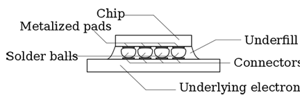
Flip chip, also known as Controlled Collapse Chip Connection or its acronym, C4, is a method for interconnecting semiconductor devices, such as IC chips and MEMS, to external circuitry with solder bumps that have been deposited onto the chip pads. The solder bumps are deposited on the chip pads on the top side of the wafer during the final wafer processing step. In order to mount the chip to external circuitry (e.g., a circuit board or another chip or wafer), it is flipped over so that its top side faces down, and aligned so that its pads align with matching pads on the external circuit, and then the solder is flowed to complete the interconnect. This is in contrast to wire bonding, in which the chip is mounted upright and wires are used to interconnect the chip pads to external circuitry.
- Process steps
- Integrated circuits are created on the wafer
- Pads are metalized on the surface of the chips
- Solder dots are deposited on each of the pads
- Chips are cut
- Chips are flipped and positioned so that the solder balls are facing the connectors on the external circuitry
- Solder balls are then remelted (typically using hot air reflow)
- Mounted chip is “underfilled” using an electrically-insulating adhesive
Comparison of mounting technologies
Wire bonding:
The interconnections in a power package are made using thick aluminium wires (250 to 400 µm) wedge-bondedIn typical semiconductor fabrication systems chips are built up in large numbers on a single large "wafer" of semiconductor material, typically silicon. The individual chips are patterned with small pads of metal near their edges that serve as the connections to an eventual mechanical carrier. The chips are then cut out of the wafer and attached to their carriers, typically with small wires (see wire bonding). These wires eventually lead to pins on the outside of the carriers, which are attached to the rest of the circuitry making up the electronic system.
Flip Chip:
The processing of a flip chip is similar to conventional IC fabrication with the addition of a few steps.[1] Near the end of the process the attachment pads are "metalized" to make them more suitable for being soldered onto. This typically consists of several treatments. A small dot of solder is then deposited on each of the pads. The chips are then cut out of the wafer as normal.
Recently high speed mounting methodology evolved through a co-operation between Reel Service Ltd. and Siemens AG in the development of a high speed mounting tape known as 'MicroTape.'[1]. By adding a tape and reel process into the assembly methodology, placement at high speed, typically 20,000 placements per hour are achievable using standard PCB assembly equipment, much to the delight of the mobile handset industry.
Advantages:
The resulting completed flip chip assembly is much smaller than a traditional carrier-based system; the chip sits directly on the circuit board, and is much smaller than the carrier both in area and height. The short wires greatly reduce inductance, allowing higher-speed signals, and also carry heat better.
Disadvantages:
Flip chips have several disadvantages as well. The lack of a carrier means they are not suitable for easy replacement, or manual installation. They also require very flat surfaces to mount to, which is not always easy to arrange, or sometimes difficult to maintain as the boards heat and cool. Also, the short connections are very stiff, so the thermal expansion of the chip must be matched to the supporting board or the connections can crack.
Link to this Webpage:
© Copyright 2000 -
2024, by Engineers Edge, LLC
www.engineersedge.com
All rights reserved
Disclaimer |
Feedback
Advertising
| Contact